Software-Defined Radio Demodulator
Background
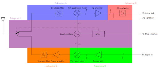
This was a project done for a second-year design course (ECE295: Hardware Design and Communication). In teams of three, we built subsystems that were assembled at the end of the course to produce a fully operational software-defined flexible radio transceiver. My team’s final result: a functional demodulator implementing the phasing method of demodulation.
Process and Design
Our design was composed of three stages: a filtering stage, an adder, and finally an audio amplifier. The filtering stage consisted of two chains of filters, which phase-shifted the input signals received from the previous subsystem to be 180 degrees apart. The adding stage summed the two phase-shifted signals to produce either a cancellation or summation of signals, depending on whether we wanted to isolate for the upper sideband or lower sideband signal. Lastly, the audio amplifier took the result of the adder and amplifies the signal to ensure it is within an audible range.
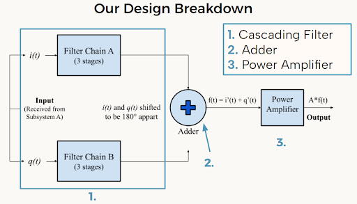
We used all-pass filters for our final design. Prior to that, we experimented with using high-pass and low-pass filters because they provide a constant phase response and it was specified within our course’s Interface Control Document that our demodulator must be functional for all frequencies between 0 to 4kHz. However, even though the phase response of our HPF/LPF chain was optimal, the magnitude response was inconsistent. We learned that even though an APF chain didn’t provide as consistent of a phase response across the necessary frequencies, it was functional for our purposes because our input signals didn’t consist of many low-frequency components.

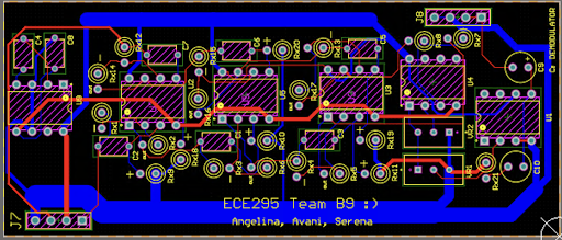
After many hours of toil, we produced the following Altium design:
Testing and Results
Success! We were able to produce a flexible (works for a wide range of input frequencies) demodulation system which outputs a signal that is audible and understandable.
Our oscilloscope results are also as expected: we get a cancellation when we isolate for the LSB (left), and we get a summation when we isolate for the USB (right).

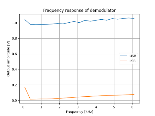
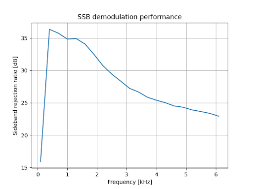
The oscilloscope only shows system outputs for one input frequency at a time. Here are some plots generated through a Python script to show the response of our PCB over a range of frequencies:
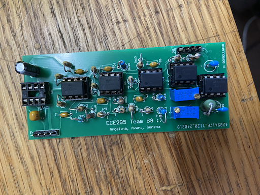
This was an incredibly fulfilling project to partake in! Here is our final PCB:
